 | –≠–ª–µ–∫—Ç—Ä–æ–Ω–Ω—ã–π –∫–æ–º–ø–æ–Ω–µ–Ω—Ç: AKD4380 | –°–∫–∞—á–∞—Ç—å:  PDF PDF  ZIP ZIP |

ASAHI KASEI
[AKD4380]
<KM061500>
'00/04
- 1 -
GENERAL DESCRIPTION
The AKD4380 is an evaluation board for AK4380, which is 96kHz sampling 24Bit
DAC.
AKD4380 has the interface with AKM's wave generator using ROM data and with AKM's A/D converter
evaluation boards. Therefore, it is easy to evaluate the AK4380. The AKD4380 also has the digital audio
interface and can achieve the interface with digital audio systems via opt-connector or RCA connector.
n
Ordering guide
AKD4380
---
Evaluation board for AK4380
FUNCTION
∑
Compatible with 2 types of interface
-Direct interface with AKM's A/D converter evaluation boards (539X,535X)
,and direct interface with a signal generator (AKD43XX)
- On-board CS8414 as DIR which accepts optical or RCA input.
∑
BNC connector for an external clock input by 10 pin Hearder.
10pin Header
E x ternal
C lo c k
R O M D a ta
o r
A /D in p u t
O p tical
In p u t
C S 8414
(DIR )
C lo c k
G e n e rato r
A K 4380
R c h
L c h
Figure 1. AKD4380 Block Diagram
Evaluation board Rev.A for AK4380
AKD4380

ASAHI KASEI
[AKD4380]
<KM061500>
'00/04
- 2 -
n
Analog output
Analog signal is output through BNC connectors on the board. And the output level of AK4380 is 3.45Vpp.
n
Operation sequence
1) Set up the power supply lines.
[VA] (red)
= 4.5
5.5V
[VD] (red)
= 4.5
5.5V
[AGND] (black)
= 0V
[DGND] (black)
= 0V
Each supply line should be distributed from the power supply unit.
2) Set up the evaluation mode, jumper pins and DIP switches.
(See the followings.)
3) Power on.
The AK4380 should be reset once bringing upon power-up
n
Evaluation mode
Applicable evaluation modes
1) DIR (Optical Link and RCA) (default)
2) Using ROM data (AK43XX)
3) Using AKM's evaluation board for ADC
4) Feeding all signals from external
1) DIR(Optical Link)
PORT3(TORX176) or J3(RCA) is used. All clock are supplied from CS8414(DIR). DIR generates MCLK,
BICK, LRCK and SDATA from the received data through optical connector (TORX176) or RCA connector.
Used for the evaluation using CD test disk. Nothing should be connected to PORT2. In case of using optical
connector (TORX176), select "OPT" on JP14(DIR/RX). In case of using RCA connector, select "RX".
JP12
MCLK
JP11
DIR
JP3
BICK
DIR
ADC
JP4
LRCK
JP10
DIR_DATA
JP9
SDTI
DIR
ADC
DIR
XTL
EXT
GND
VD
DATA
GND
JP13
XTE
2) Ideal sine wave generated by ROM data
Connect the AKD43XX with PORT2(ADC/ROM). AKD4380 sends MCLK to AKD43XX, and receives LRCK,
BICK and SDATA. In case of using external master clock through a BNC connector, select "BNC" on
JP12(MCLK) and short JP13(XTE).
JP12
MCLK
JP11
DIR
JP3
BICK
DIR
ADC
JP4
LRCK
JP10
DIR_DATA
JP9
SDTI
DIR
ADC
DIR
XTL
EXT
GND
VD
DATA
GND
JP13
XTE
ASAHI KASEI
[AKD4380]
<KM061500>
'00/04
- 3 -
3) Using AKM's evaluation board for ADC
To evaluate AK4380 with analog input, the AKM's evaluation board for ADC can be used. MCLK, BICK and
LRCK are supplied from clock generator on the AKD4380, and analog signal is A/D converted and send to
AKD4380 through PORT2(ADC/ROM). In case of using external master clock through a BNC connector, select
"BNC" on JP12(MCLK) and short JP13(XTE).
JP12
MCLK
JP11
DIR
JP3
BICK
DIR
ADC
JP4
LRCK
JP10
DIR_DATA
JP9
SDTI
DIR
ADC
DIR
XTL
EXT
GND
VD
DATA
GND
JP13
XTE
4) Feeding all signals from external
Under the following set-up, all external signals can be fed through POTR2.
JP12
MCLK
JP11
DIR
JP3
BICK
DIR
ADC
JP4
LRCK
JP10
DIR_DATA
JP9
SDTI
DIR
ADC
DIR
XTL
EXT
GND
VD
DATA
GND
JP13
XTE
n
Clock (MCLK,BICK,LRCK) set up
In case of using evaluation mode 1), JP9,10 and 17 should be set up as follows.
They need no care for other evaluation mode.
MCLK
JP5
(X_MCLK)
JP8
(X_LRCK)
BICK
JP7
(X_BICK)
128fs
256/128
LR_128
32fs
64fs
64fs/32fs
128fs/64fs
256fs
256/128
LR_256/512
32fs
64fs
128fs
32fs
64fs/32fs
128fs/64fs
default
512fs
512
LR_256/512
32fs
64fs
128fs
32fs
64fs/32fs
128fs/64fs
Table 1. Clock set up

ASAHI KASEI
[AKD4380]
<KM061500>
'00/04
- 4 -
PORT1
up-I/F
1
2
9
10
CSN
CCLK
CDTI
n
DIP switch set up
[SW4](MODE1): No.1 to 2 set the mode of AK4380 and No.3 to 5 set the mode of CS8414.
No.
Pin
OFF
ON
1
DFS0
Normal speed
Double speed
2
DIF0
24bit, MSB justified
I2S
3
M2
4
M1
5
M0
Digital interface format of CS8414
(See table 4.)
(Note)
Table 2. SW3 set-up
(Note:
M2-0 should be selected at only evaluation mode 1.
In other mode, these should be "OFF".)
3
4
5
6
7
8
JP6
Mode
Format
DIF0
DIF1
DIF2
M2
M1
M0
BICK2
0
16bit, LSB justified
0
0
0
1
0
1
THR
1
20bit, LSB justified
1
0
0
-
-
-
-
2
24bit, MSB justified
0
1
0
0
0
0
INV
3
I2S
1
1
0
0
1
0
THR
default
4
24bit, LSB justified
0
0
1
-
-
-
-
Table 3. Digital interface format set-up (1=ON, 0=OFF)
(CS8414 does not correspond to 20/24bit LSB justified format.)
n
Other jumper pins set up
[JP1] (GND): Analog ground and digital ground
open:
separated <default>
short: AGND and DGND are connected.
[JP2] (DZF) Mute circuit
ON: Used . Analog output are muted when DZF="H".
OFF: Not used. <default>
[JP6] (BICK_ PHASE): Phase of BCLK
THR:
BICK is coincides with AK4380. <default>
INV:
BICK is inverted.
n
The function of the toggle SW.
[SW1](PDN):
Resets the AK4380. Keep "H" during normal operation.
[SW2](SMUTE):
Soft mute of AK4380. Bring "H" when using soft mute.
[SW3](P/S): H: parallel mode.
L: serial mode.
n
Indication for LED
[LED1] (VERF):
Monitor VERF pin of the CS8414. LED turns on when some error has occurred to CS8414.
[LED2]: (PREM): Indicate whether the input data of CS8414 is pre-emphasized or not.
n
Serial control mode
The AK4380 can be controlled via the printer port (parallel port) of IBM-AT
compatible PC. Connect PORT1(up-I/F) with PC by 10-line flat cable
packed with the AKD4380.
Take care of the direction of connector. There is a mark at 1pin.
The pin layout of PORT1 is as Figure 2.
Figure 2. PORT1 pin layout

ASAHI KASEI
[AKD4380]
<KM061500>
'00/04
- 5 -
MEASUREMENT RESULTS
[Measurement condition]
∑
Measurement unit : Audio Precision System Two Cascade
∑
MCLK
: 256fs
∑
BICK
: 64fs
∑
fs
: 44.1kHz, 96kHz
∑
BW
: 10Hz
20kHz (fs=44.1kHz), 10Hz
40kHz (fs=96kHz)
∑
Bit
: 24bit
∑
Power Supply
: VDD=5V
∑
Interface
: DIR (fs=44.1kHz, 96kHz)
∑
Temperature
: Room
Parameter
Input signal
Measurement filter
fs=44.1kHz
S/(N+D)
1kHz, 0dB
20kLPF
94.0dB
22kLPF
97.2dB
DR
1kHz, -60dB
22kLPF, A-weighted
100.0dB
22kLPF
97.2dB
S/N
no signal
22kLPF, A-weighted
100.0dB
Parameter
Input signal
Measurement filter
fs=96kHz
S/(N+D)
1kHz, 0dB
40kLPF
92.3dB
40kLPF
94.5dB
DR
1kHz, -60dB
22kLPF, A-weighted
97.2dB
40kLPF
94.5dB
S/N
no signal
22kLPF, A-weighted
97.2dB
ASAHI KASEI
[AKD4380]
<KM061500>
'00/04
- 6 -
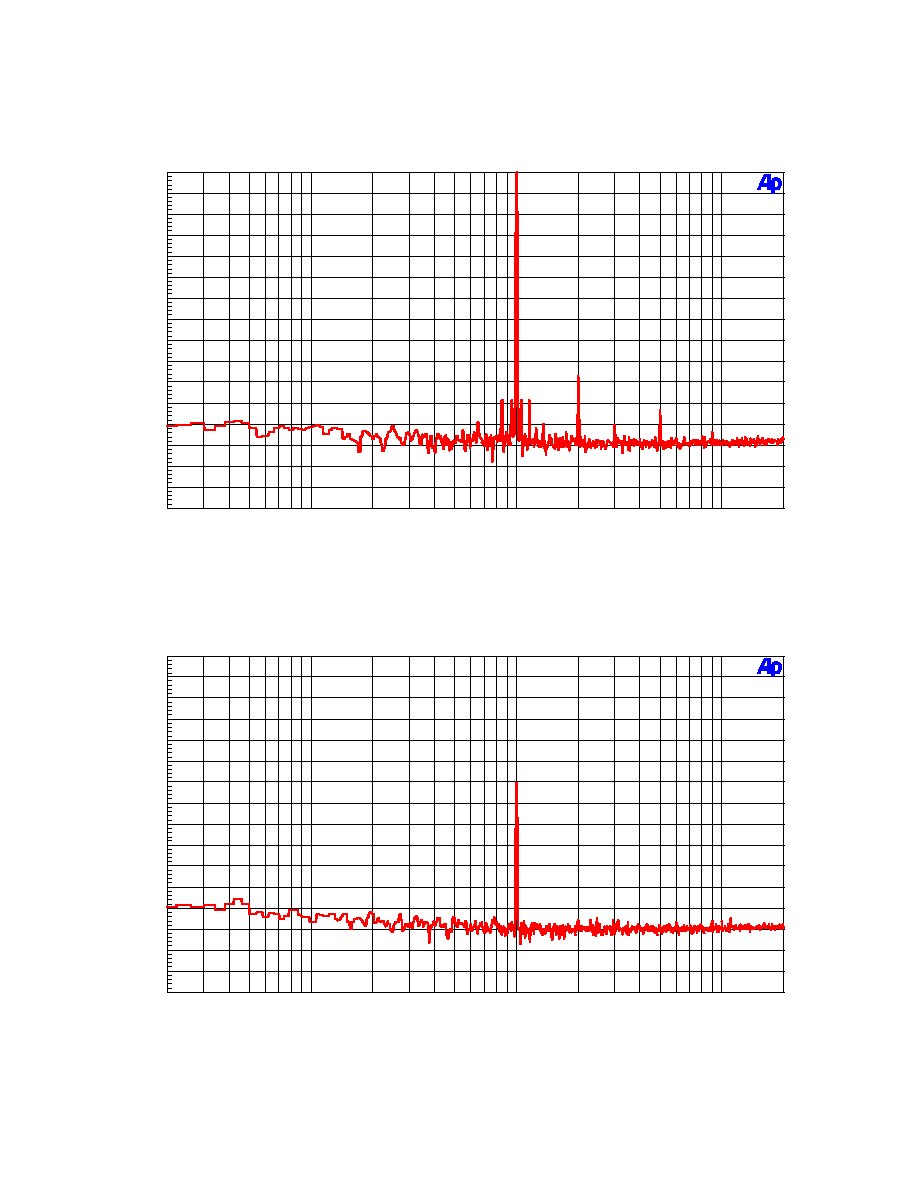
(fs=44.1kHz)
A K M
A K 4 3 8 0 R e v.A F F T (Input=0dBFS, fin=1kHz)
-160
+ 0
-150
-140
-130
-120
-110
-100
-90
-80
-70
-60
-50
-40
-30
-20
-10
d
B
r
A
20
20k
50
100
200
500
1k
2k
5k
10k
Hz
A K M
A K 4 3 8 0 R e v.A F F T (Input=-60dBFS, fin=1kHz)
-160
+ 0
-150
-140
-130
-120
-110
-100
-90
-80
-70
-60
-50
-40
-30
-20
-10
d
B
r
A
20
20k
50
100
200
500
1k
2k
5k
10k
Hz
ASAHI KASEI
[AKD4380]
<KM061500>
'00/04
- 7 -
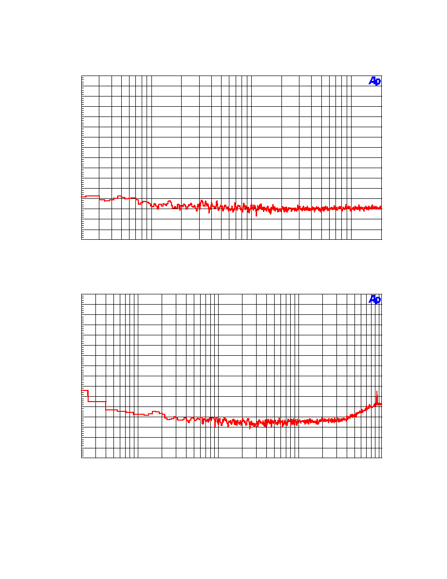
(fs=44.1kHz)
A K M
A K 4 3 8 0 R e v.A F F T (Input="0"data, fin=1kHz)
-160
+ 0
-150
-140
-130
-120
-110
-100
-90
-80
-70
-60
-50
-40
-30
-20
-10
d
B
r
A
20
20k
50
100
200
500
1k
2k
5k
10k
Hz
A K M
A K 4 3 8 0 R e v.A F F T (Input="0"data, fin=1kHz, HiB W )
-160
+ 0
-150
-140
-130
-120
-110
-100
-90
-80
-70
-60
-50
-40
-30
-20
-10
d
B
r
A
20
100k
50
100
200
500
1k
2k
5k
10k
20k
50k
Hz
ASAHI KASEI
[AKD4380]
<KM061500>
'00/04
- 8 -
(fs=44.1kHz)
A K M
A K 4 3 8 0 R e v.A T HD + N vs Amplitud e (fin=1kHz)
-150
+ 0
-140
-130
-120
-110
-100
-90
-80
-70
-60
-50
-40
-30
-20
-10
dBFS
-110
-70
-108
-106
-104
-102
-100
-98
-96
-94
-92
-90
-88
-86
-84
-82
-80
-78
-76
-74
-72
d
B
r
A
A K M
A K 4 3 8 0 R e v.A T HD + N vs Input Frequency (fin=1kHz)
20
20k
50
100
200
500
1k
2k
5k
10k
Hz
-110
-70
-108
-106
-104
-102
-100
-98
-96
-94
-92
-90
-88
-86
-84
-82
-80
-78
-76
-74
-72
d
B
r
A

ASAHI KASEI
[AKD4380]
<KM061500>
'00/04
- 9 -
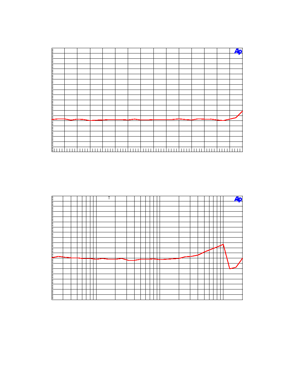
A K M
A K 4 3 8 0 R e v.A L inearity
-150
+ 0
-140
-130
-120
-110
-100
-90
-80
-70
-60
-50
-40
-30
-20
-10
dBFS
-150
+ 0
-140
-130
-120
-110
-100
-90
-80
-70
-60
-50
-40
-30
-20
-10
d
B
r
A
A K M
A K 4 3 8 0 R e v.A F requency Response
2k
20k
4k
6k
8k
10k
12k
14k
16k
18k
Hz
-0.5
+0.5
-0.45
-0.4
-0.35
-0.3
-0.25
-0.2
-0.15
-0.1
-0.05
+ 0
+0.05
+0.1
+0.15
+0.2
+0.25
+0.3
+0.35
+0.4
+0.45
d
B
r
A

ASAHI KASEI
[AKD4380]
<KM061500>
'00/04
- 10 -
(fs=44.1kHz)
A K M
A K 4 3 8 0 R e v.A C rosstalk
40
40k
50
100
200
500
1k
2k
5k
10k
20k
Hz
-120
-70
-117.5
-115
-112.5
-110
-107.5
-105
-102.5
-100
-97.5
-95
-92.5
-90
-87.5
-85
-82.5
-80
-77.5
-75
-72.5
d
B
r
A

ASAHI KASEI
[AKD4380]
<KM061500>
'00/04
- 11 -
(fs=96kHz)
A K M
A K 4 3 8 0 R e v.A F F T (Input=0dBFS,fin=1kHz)
40
40k
50
100
200
500
1k
2k
5k
10k
20k
Hz
-160
+ 0
-150
-140
-130
-120
-110
-100
-90
-80
-70
-60
-50
-40
-30
-20
-10
d
B
r
A
A K M
A K 4 3 8 0 R e v.A F F T (Input=-60dBFS,fin=1kHz)
40
40k
50
100
200
500
1k
2k
5k
10k
20k
Hz
-160
+ 0
-150
-140
-130
-120
-110
-100
-90
-80
-70
-60
-50
-40
-30
-20
-10
d
B
r
A

ASAHI KASEI
[AKD4380]
<KM061500>
'00/04
- 12 -
(fs=96kHz)
A K M
A K 4 3 8 0 R e v.A F F T (Input="0"data,fin=1kHz)
40
40k
50
100
200
500
1k
2k
5k
10k
20k
Hz
-160
+ 0
-150
-140
-130
-120
-110
-100
-90
-80
-70
-60
-50
-40
-30
-20
-10
d
B
r
A

ASAHI KASEI
[AKD4380]
<KM061500>
'00/04
- 13 -
(fs=96kHz)
A K M
A K 4 3 8 0 R e v.A T HD + N vs Amplitud e(fin=1kHz)
-150
+ 0
-140
-130
-120
-110
-100
-90
-80
-70
-60
-50
-40
-30
-20
-10
dBFS
-110
-70
-108
-106
-104
-102
-100
-98
-96
-94
-92
-90
-88
-86
-84
-82
-80
-78
-76
-74
-72
d
B
r
A
A K M
A K 4 3 8 0 R e v.A T HD + N vs Input Frequency(Input=0dBFS)
40
40k
50
100
200
500
1k
2k
5k
10k
20k
Hz
-110
-70
-108
-106
-104
-102
-100
-98
-96
-94
-92
-90
-88
-86
-84
-82
-80
-78
-76
-74
-72
d
B
r
A

ASAHI KASEI
[AKD4380]
<KM061500>
'00/04
- 14 -
(fs=96kHz)
A K M
A K 4 3 8 0 L inearity
-150
+ 0
-140
-130
-120
-110
-100
-90
-80
-70
-60
-50
-40
-30
-20
-10
d
B
r
A
-150
+ 0
-140
-130
-120
-110
-100
-90
-80
-70
-60
-50
-40
-30
-20
-10
dBFS
A K M
A K 4 3 8 0 R e v.A F requency Response
2.5k
40k
5k
7.5k
10k
12.5k
15k
17.5k
20k
22.5k
25k
27.5k
30k
32.5k
35k
37.5k
Hz
-0.5
+0.5
-0.45
-0.4
-0.35
-0.3
-0.25
-0.2
-0.15
-0.1
-0.05
+ 0
+0.05
+0.1
+0.15
+0.2
+0.25
+0.3
+0.35
+0.4
+0.45
d
B
r
A

ASAHI KASEI
[AKD4380]
<KM061500>
'00/04
- 15 -
A K M
A K 4 3 8 0 R e v.A C rosstalk
40
40k
50
100
200
500
1k
2k
5k
10k
20k
Hz
-120
-70
-117.5
-115
-112.5
-110
-107.5
-105
-102.5
-100
-97.5
-95
-92.5
-90
-87.5
-85
-82.5
-80
-77.5
-75
-72.5
d
B
r
A
5
5
4
4
3
3
2
2
1
1
D
D
C
C
B
B
A
A
H
Analog Ground
Digital Ground
for 74HCU04,74AC74 ,
74HC14, 74HC4040
CSN
CDTI
CCLK
L
H
DFS
DIF0
M0
M1
M2
P
S
AK4380
A
AKD4380
A3
1
2
Monday, September 27, 1999
Title
Size
Document Number
Rev
Date:
Sheet
of
MCLK
BICK
SDTI
LRCK
AOUTL
AOUTR
DZF
P/S
M0
SMUTE
M2
P/S
M1
SMUTE
VA2
DIR_VD
VD
VA
VD
VD
VD
VD
VD
D1
SW1
PDN
R9
220
R1
220
JP1
GND
R4
10k
U3B
74HC14
3
4
R8
(short)
R7
(short)
R6
(short)
R5
(short)
R3
(short)
+
C25
10u
+
C12
10u
U2
74HC541
2
3
4
5
6
7
8
9
1
19
18
17
16
15
14
13
12
11
A1
A2
A3
A4
A5
A6
A7
A8
G1
G2
Y1
Y2
Y3
Y4
Y5
Y6
Y7
Y8
R13
2.2k
PORT1
uP-I/F
10
8
6
4
2
1
3
5
7
9
R15
51
U4
74HC157
2
3
5
6
11
10
14
13
1
15
4
7
9
12
1A
1B
2A
2B
3A
3B
4A
4B
A/B
G
1Y
2Y
3Y
4Y
R16
51
R11
2.2k
R12
2.2k
R14
51
U3A
74HC14
1
2
C13
0.1u
C1
0.1u
C2
0.1u
C3
0.1u
C4
0.1u
+
C5
47u
D2
SW2
SMUTE
R17
10k
U3E
74HC14
11
10
U3F
74HC14
13
12
C14
0.1u
U3C
74HC14
5
6
U3D
74HC14
9
8
L2
10u
1
2
RP1
47K
5
4
3
2
1
SW4
MODE
1
2
3
4
5
10
9
8
7
6
L1
(short)
1
2
R2
27k
+
C9
10u
C10
0.1u
+
C6
47u
R10
27k
C11
0.1u
+
C8
10u
SW3
P/S
AK4380
U1
1
2
3
4
5
6
7
8
10
11
12
15
14
13
16
9
MCLK
BICK
SDTI
LRCK
PDN
CSN/SMUTE
CCLK/DFS
CDTI/DIF0
AOUTR
AOUTL
VCOM
VREF
VDD
VSS
DZF
P/S

5
5
4
4
3
3
2
2
1
1
D
D
C
C
B
B
A
A
VD
GND
RX
OPT
AD/ROM
SDATA
MCLK
LRCK
BICK
THR
INV
XTL
BN
C
DIR
32fs
64fs/32fs
128fs/64fs
ADC
DIR
DIR
ADC
DA
TA
G
N
D
ON
OFF
(10k,10k)
(10k,10k)
LR_256/512
LR_128
256/128
512
Interface
A
AKD4380
A3
2
2
Thursday, October 14, 1999
Title
Size
Document Number
Rev
Date:
Sheet
of
X_BICK
DIR_LRCK
LRCK
BICK
M0
M2
X_BICK
M1
SDTI
DIR_BICK
X_LRCK
VA2
DZF
AOUTL
AOUTR
X_LRCK
DIR_BICK
DIR_LRCK
MCLK
DIR_VD
VD
VD
VD
VD
VD
U6C
74HCU04
5
6
R22
1k
JP10
DIR_DATA
R24
1k
R23
1M
U6F
74HCU04
13
12
U6D
74HCU04
9
8
U6E
74HCU04
11
10
R20
10k
JP11
DIR
1
2
3
L4
47u
1
2
X1
11.2896MHz
1
2
JP3
LRCK
JP4
BICK
R18
10k
JP2
DZF
TR1
RN1202
1
3
2
TR3
2SC3327
1
3
2
J1
AOUTL
R19
10k
J2
AOUTR
TR4
2SC3327
1
3
2
U6A
74HCU04
1
2
JP6
BICK_PHASE
1
2
3
JP12
MCLK
JP8
X_LRCK
LED1
VERF
2
1
LED2
PREM
2
1
J3
RCA
R26
75
U7A
74AC74
2
3
5
6
4
1
D
CLK
Q
Q
PR
CL
JP7
X_BICK
C21
0.01u
PORT3
TORX176
1
3
4
2
6
5
OUT
VCC
GND
GND
6
5
U8
CS8414
1
2
3
4
5
6
7
8
9
10
11
12
13
14
15
16
17
18
19
20
21
22
23
24
25
26
27
28
C
Cd/F1
Cc/F0
Cb/E2
Ca/E1
C0/E0
VD+
DGND
RXP
RXN
FSYNC
SCK
CS12/FCK
U
CBL
SEL
M3
M2
MCK
FILT
AGND
VA+
M0
M1
ERF
SDATA
Ce/F2
VREF
C23
0.01u
C22
0.1u
PORT2
ADC/ROM
1
2
3
4
5
6
7
8
9
10
R25
1k
+
C15
10u
U6B
74HCU04
3
4
C18
0.1u
JP9
SDTI
1
2
3
JP13
XTE
JP14
DIR/RX
1
2
3
L3
10u
1
2
R27
51
U5
74HC4040
10
11
9
7
6
5
3
2
4
13
12
14
15
1
CLK
RST
Q1
Q2
Q3
Q4
Q5
Q6
Q7
Q8
Q9
Q10
Q11
Q12
J4
BNC
C19
(open)
C20
(open)
TR2
RN2202
1
3
2
U7B
74AC74
12
11
9
8
10
13
D
CLK
Q
Q
PR
CL
C16
0.1u
R21
1k
+
C17
10u
C24
47n
JP5
X_MCLK


IMPORTANT NOTICE
∑
These products and their specifications are subject to change without notice. Before considering any
use or application, consult the Asahi Kasei Microsystems Co., Ltd. (AKM) sales office or authorized
distributor concerning their current status.
∑
AKM assumes no liability for infringement of any patent, intellectual property, or other right in the
application or use of any information contained herein.
∑
Any export of these products, or devices or systems containing them, may require an export license or
other official approval under the law and regulations of the country of export pertaining to customs and
tariffs, currency exchange, or strategic materials.
∑
AKM products are neither intended nor authorized for use as critical components in any safety, life
support, or other hazard related device or system, and AKM assumes no responsibility relating to any
such use, except with the express written consent of the Representative Director of AKM. As used
here:
(a) A hazard related device or system is one designed or intended for life support or maintenance of
safety or for applications in medicine, aerospace, nuclear energy, or other fields, in which its failure
to function or perform may reasonably be expected to result in loss of life or in significant injury or
damage to person or property.
(b) A critical component is one whose failure to function or perform may reasonably be expected to
result, whether directly or indirectly, in the loss of the safety or effectiveness of the device or system
containing it, and which must therefore meet very high standards of performance and reliability.
∑
It is the responsibility of the buyer or distributor of an AKM product who distributes, disposes of, or
otherwise places the product with a third party to notify that party in advance of the above content and
conditions, and the buyer or distributor agrees to assume any and all responsibility and liability for and
hold AKM harmless from any and all claims arising from the use of said product in the absence of such
notification.